0
$\begingroup$

I am trying to learn more about the CPU in embedded systems. As I am studying I learned that the IR (Instruction Register) is kind of a special register.

What I would like to know is how to know the width / size of the IR. So, what I mean is for e.g. if I have a 16-bits CPU with 18 address lines (that means max. 256 Kbyte addressable memory). What is the width of the IR of this CPU? In this example the size of opcode are not given. Is it important to know how many opcodes there are. But if it does matter the size of opcodes is maximum 1 byte.

Could someone give me some insight of how this works.

Thank you.

$\endgroup$

1 Answer 1

1
$\begingroup$

In a typical scalar in-order issue microcontroller, the instruction register holds however many bits are needed to control the data path.

Modern microcontrollers are typically Harvard architectures, with program memory stored in flash, with a modest amount of data/read-write memory on-chip. This means that, unlike traditional scalar CPUs, the bus width of program memory and the bus width of data memory does not have to be the same.

Microcontroller instruction sets are typically designed so that the instruction as a whole can be understood from the first word fetched from flash. Any additional words contain data only, and hence do not need to participate in instruction decoding.

As an example, here is the AVR block diagram from a data sheet that I picked at random:
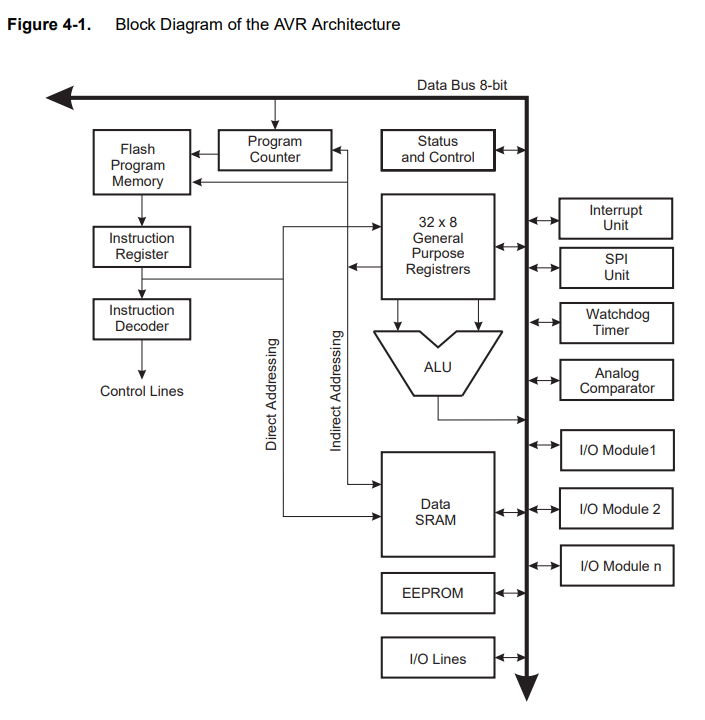
AVR core block diagram

The instruction register holds whatever comes out of program memory. Since AVR has 16-bit instructions, we would expect it to be a 16-bit register.

Now consider the PIC instruction set. Different models have different instruction sizes, anything from 12 bit to 16 bit. Modern microcontrollers can handle this just fine because, as noted earlier, instruction memory can have a different word size from data memory. This instruction word contains all of the information needed to understand what the instruction needs to do, so this is the size of the instruction register.

A mid-range core PIC has a 14-bit instruction word, so it will almost certainly have a 14-bit instruction register. And if you look at a data sheet, this turns out to be correct, and is even labelled on the diagram:
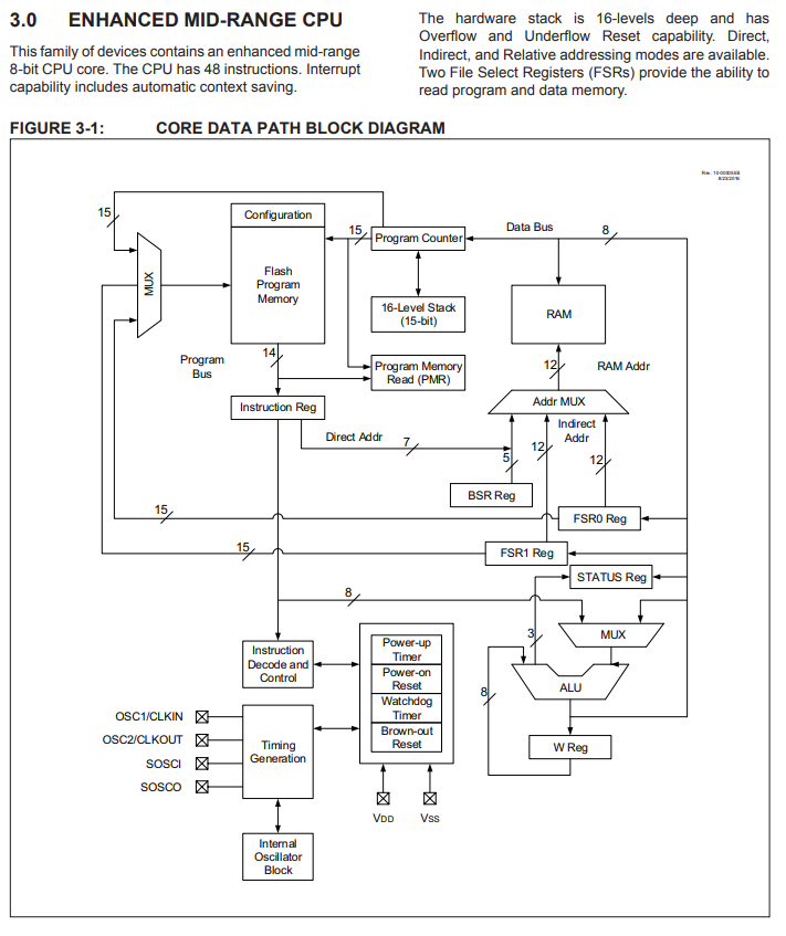
Enhanced mid-range PIC block diagram

So in summary: On a typical modern microcontroller, the IR size is one word of program memory, and the instruction encoding is carefully designed so that this word contains all the information that instruction decoding needs.

$\endgroup$
5
  • $\begingroup$ I am a little confused, and I hope you can clarify it. The AVR example that you have mentioned has around 131 instructions. I have checked it in the datasheet and on the first page it is mentioned: "131 Powerful Instructions – Most Single Clock Cycle Execution". 131 instructions can fit easily into 8-bits, because 2^8=256 (and 2^7=128 too less) so 8-bits instruction. What I don't understand is that some of these instructions need a memory address to hold as an operand. How do the CPU handle this? Because the IR size is 16-bits but it only has 8-bits instructions. Thank you. $\endgroup$
    – Karl M
    Commented Dec 7, 2020 at 10:23
  • $\begingroup$ So let's take a two-word instruction such as CALL as our example. The second word of that instruction is pure data. So the control signals within the CPU core can be generated entirely from the first word, which can be held in the IR until the instruction has completed. It doesn't make a lot of sense to compress all 16 bits of the instruction word into an 8-bit opcode only to decompress it into individual control signals again later. It might help to look at a more detailed diagram, such as the famous 6502 block diagram from this paper: projects.ncsu.edu/wcae//WCAE1/hanson.pdf $\endgroup$
    – Pseudonym
    Commented Dec 7, 2020 at 12:01
  • $\begingroup$ The interesting part is the decode logic which takes up most of the left-hand side of the diagram. Ignore the predecode register and predecode logic; that is only there for pipelining and interrupt handling. The ultimate result of instruction decoding is the few dozen single-bit control lines coming out of "random control logic". This (as well as the "decode ROM", which is actually a PLA) is combinational logic whose inputs are the IR and various timing/control flip-flops. This is much easier to generate from the IR than from reduced set of opcodes. $\endgroup$
    – Pseudonym
    Commented Dec 7, 2020 at 12:11
  • $\begingroup$ I understand that the most interesting part is decoding the IR. That is the part where it makes sense for the CPU what to do with the instruction. What I understand from your comment is that CALL is a 2-word instruction. The first word is the instruction and the second word is pure data. So, does this mean that it takes one more cycle? Because, first it decodes the instruction than it sees that it needs an operand. It fetches the operand (pure data) into the IR and then it can execute the instruction? Am I correct? I appreciate the help you are offering. $\endgroup$
    – Karl M
    Commented Dec 7, 2020 at 12:21
  • $\begingroup$ I have found one example I want to show you see: ww1.microchip.com/downloads/en/devicedoc/… on page 19, 2.11 Direct Programming Addressing, JMP and CALL. It shows that it splits it in parts: first part OP, second part 6 MSB. And the second cycle it fetches 16 LSB. After that it executes the instruction and puts the data into the PC. $\endgroup$
    – Karl M
    Commented Dec 7, 2020 at 12:31

Your Answer

By clicking “Post Your Answer”, you agree to our terms of service and acknowledge you have read our privacy policy.

Not the answer you're looking for? Browse other questions tagged or ask your own question.